The Selection and Application of FETs
Author: Shenzhen Yuan Zhi Electronics Co., Ltd.Time:2018-03-01 17:15:45Views:2691【SML】
FET widely used in analog circuits and digital circuits, and our lives are inseparable. The advantages of FETs are: First, the drive circuit is relatively simple. FETs
require much less drive current...
label:
FET widely used in analog circuits and digital circuits, and our lives are inseparable. The advantages of FETs are: First, the drive circuit is relatively simple. FETs
require much less drive current than BJTs and can typically be driven
directly by CMOS or open-collector TTL driver circuits; second, FETs
switch faster and can operate at higher speeds because there is no
charge Storage
effect; In addition there is no secondary breakdown FET breakdown
failure mechanism, it is often higher endurance at higher temperatures,
and the possibility of thermal breakdown lower, but also in a wide
temperature range can provide better performance. FETs have found numerous applications in consumer electronics,
industrial products, electromechanical devices, smartphones and other
portable digital electronics.
In
recent years, with the rapid development of the field application of
FET products such as automobile, communication, energy, consumer and
green industry in recent years, the power FET is attracting much
attention. It is predicted that China's power MOSFET market in 2010-2015 overall compound annual growth rate will reach 13.7%. Although
iSuppli, a market research firm, said power FET markets will slow this
year as a result of macro-investment and economic policies and the
supply of wafers and raw materials due to the earthquake in Japan,
demand for consumer electronics and data processing remains strong and
long-term From the point of view, the power FET growth will continue for a long period of time.
Technology has been progressing, power FET market has been gradually challenged by new technologies. For
example, many companies in the industry have already started to develop
GaN power devices, and the space for asserting the performance gains of
silicon power FETs has been very limited. However,
GaN power MOSFET market challenge is still in its infancy, FET
technology maturity, supply and other aspects still occupy a clear
advantage, after more than three decades of development, FET market is
not Will be quickly replaced by new technology.
In five years or even longer, the FET will still dominate. FET
will continue to be the first time that many new engineers will come
into contact with the device, this issue will start from the foundation
to explore some of the basics of FET, including selection, introduction
of key parameters, system and cooling considerations For everyone to do some introduction.
One. The basis of FET selection
There are two types of FETs: N-channel and P-channel. In power systems, FETs can be thought of as electrical switches. When a positive voltage is applied between the gate and the source of an N-channel FET, the switch is turned on. When conducting, the current can flow from the drain to the source via the switch. There is an internal resistance between the drain and the source, called the on-resistance RDS (ON). It must be clear that the gate of the FET is a high-impedance end, so always add a voltage to the gate. If
the gate is left floating, the device will not function as designed and
may turn on or off at inappropriate times, causing potential power loss
in the system. When
the voltage between the source and the gate is zero, the switch is
turned off and current stops flowing through the device. Although the device is off at this time, there is still a slight current, which is called the leakage current, IDSS.
As the basic components of the electrical system, engineers how to make the right choice based on parameters? This article will discuss how to choose the right FET in four steps.
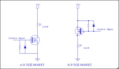
1) The choice of channel. The first step in choosing the right device for a design is to decide whether to use N-channel or P-channel FETs. In
a typical power application, when one FET is grounded and the load is
connected to mains voltage, the FET forms the LV switch. In
low-side switches, N-channel field effect transistors should be used
because of the voltage required to turn off or turn on the device. When the FET is connected to the bus and the load is grounded, it is necessary to use the high side switch. P-channel FETs are often used in this topology because of voltage-driven considerations.
2) Voltage and current selection. The higher the rated voltage, the higher the cost of the device. According to practical experience, the rated voltage should be greater than the main line voltage or bus voltage. In order to provide adequate protection so that the FET will not fail. In the case of FETs, one must determine the larger voltage that the drain-to-source can withstand, a large VDS. Other
safety factors designers need to consider include voltage transients
induced by switching electronics such as motors or transformers. The voltage ratings vary for different applications; typically 20 V
for portable devices, 20-30 V for FPGA power, and 450-600 V for 85-220
VAC applications.
In continuous conduction mode, the FET is in steady state, at which point current continues to pass through the device. Pulse spikes refer to a large number of surges (or spikes) flowing through the device. Once you have determined the current under these conditions, simply select the device that will withstand this high current.
3) Calculate the conduction loss. The
power dissipation of a FET device can be calculated by Iload2 × RDS
(ON). As the on-resistance changes with temperature, the power
dissipation changes proportionally. For
portable designs, it is easier (more common) to use lower voltages,
while for industrial designs, higher voltages can be used. Note that the RDS (ON) resistance increases slightly with current. A variety of electrical parameters on the RDS (ON) resistance can be found in the manufacturer's supplied technical data sheets.
Need
to remind designers, in general, MOS tube specification Id current is
the larger the normal current of the MOS chip, the actual use of the
larger normal current but also by the larger package current limit. Therefore, when designing a product, the larger current setting needs to consider the larger current limit of the package. It is more important to recommend the customer to design a product
using the current setting is more important to consider the internal
resistance of MOS tube parameters.
4) calculate the system's cooling requirements. Designers must consider two different situations, namely bad situations and real situations. It
is recommended that calculations be made for bad situations because
this result provides greater safety margin to ensure that the system
will not fail. In the FET data sheet there are some measurements need to be aware
of; for example, the thermal resistance between the semiconductor
junction of the packaged device and the environment, and a larger
junction temperature.
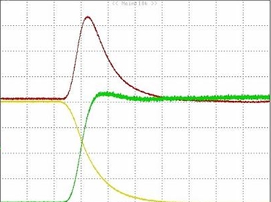
Switch loss is actually a very important indicator. As can be seen from the figure below, the product of voltage and current at the moment of conduction is quite large. To some extent determines the switching performance of the device. However,
if the system requires relatively high switching performance, a power
MOSFET with a small gate charge, QG, can be chosen.
2018-03-01
2691People browsing


 Mobile website
